Project Frankenmill – Part 33, Claustrophobia
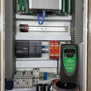
Final positions for the DIN rails and wire management have been nailed down. It’s much more tight than one should really wire a panel like this, but…
Project Frankenmill – Part 32, You’re Gonna Need a Bigger Boat
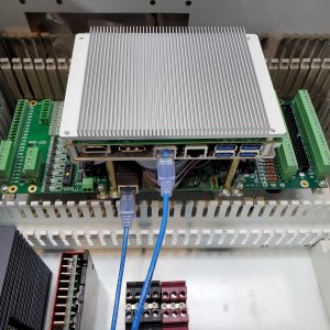
It seems to be a rule that no matter what size electronics enclosure you have, you will always have at least 10% more stuff that you need…
Project Frankenmill – Part 31, Full Pull
While I still haven’t gotten into the detail of squaring and tramming, I’ve been intensely curious to see if the new Z axis would be happier with…

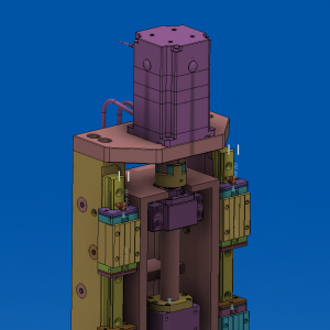
Project Frankenmill – Alpha and Omega
Since 2009, I’ve been messing around with CNC machines. I started out with a small manual milling machine from Grizzly, and converted it to CNC using a…
Project Frankenmill – Part 30, Do You Even Lift Bro?
Hauled the column back down to the shop and mounted it back on the machine. Sure is a lot heavier than it used to be! Muscling things…
Project Frankenmill – Part 29, More Machining and Motion
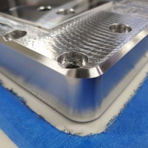
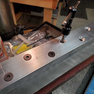
Had some productive time in the shop during the holiday. First step was to make the counterbores for the M6 cap screws a bit deeper. Easy to…
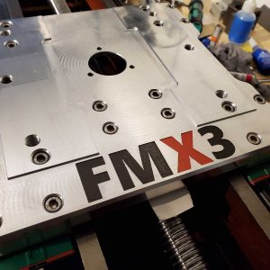
Project Frankenmill – Part 28, The Home Stretch
I used the “saw” feature of the Protomax waterjet to cut stock to rough size for the head mounting plate the other night. At the moment we…
Project Frankenmill – Part 27, So Shiny
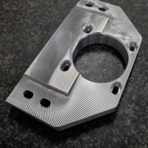
Had some time the other evening to do the final machining on the new stepper mount, on the Tormach 1100. Being able to rough cut it on…
Project Frankenmill – Part 26, Wicked Waterjet Work
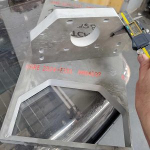
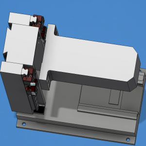
Now onto making the stepper mounting plate for the new Z axis stepper motor. We recently got a fun new toy at our makerspace, a ProtoMax waterjet….
Project Frankenmill – Part 25, Moving and Grooving
The original CNC conversion had a NEMA23 stepper located on the bottom of the column, driven by a timing belt and pulleys with a 2:1 ratio. I’m…
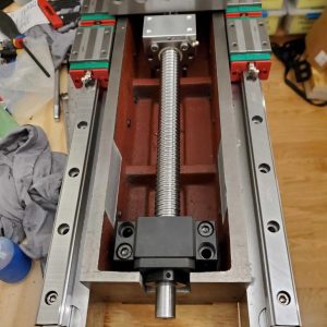
Project Frankenmill – Part 24, We’re Screwed
I considered re-using the original Thomson 16mm 0.200″ pitch ball screw from my original CNC conversion kit, but the ball nut wasn’t sounding particularly good after the…
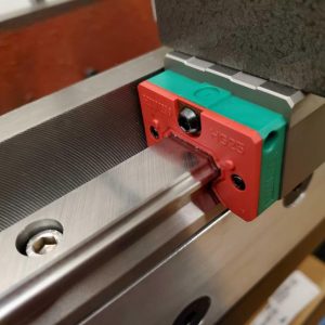
Project Frankenmill – Part 23, Rails Without Fails
Now on to the critical milling to create the mounting surfaces and reference edges for the linear rails. First thing in the morning, I spent a ton…
Project Frankenmill – Part 22, Taken for Granite
For extra security, I decided to epoxy the side bars to the column so they would not move. I figured the epoxy would also help fill in…
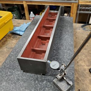
Project Frankenmill – Part 21, Milling and Drilling
Drops from the metal yard have arrived – 1.5″ x 2.5″ 2024 bar stock, and a 1″ thick chunk of 2024 plate for the Z saddle. With…
Project Frankenmill – Part 20, Choose Wisely
I mainly considered two approaches to mounting rails to the column. Approach 1 – add some kind of additional side supports to the existing column and mount…